
Amid the booming wave of the semiconductor industry, Ningbo Chengda Precision Machinery Co., Ltd. has been constantly writing new chapters of innovation. Recently, the company has made significant breakthroughs in technological cooperation and core product research and development, leading the industry's innovation direction and attracting much attention.
Ningbo Chengda Precision Machinery Co., Ltd. signed a contract with the Ningbo Institute of Materials Technology and Engineering, Chinese Academy of Sciences, to jointly establish the "Advanced Laser Processing Technology Joint Laboratory for Semiconductor Matrix Materials", and the two sides will carry out in-depth cooperation. Relying on the Laser Extreme Manufacturing Research Center led by Academician Li Lin of Ningbo Institute of Materials Technology and Engineering and its high-end talent and technological advantages, in collaboration with Chengda Precision Machinery, the two sides will focus on collaborative research and development in the field of wafer processing in integrated circuit manufacturing, and jointly build a globally leading advanced laser processing innovation and R&D platform. The two sides have joined hands with the aim of overcoming the core processing technology and equipment challenges of semiconductor matrix materials, achieving the industrialization and wide application of related technologies, and injecting strong impetus into enhancing the independent control capabilities of China's semiconductor industry.
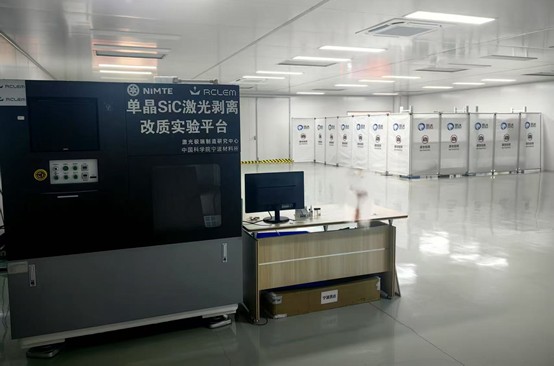
Figure 1: Joint Laboratory for Advanced Laser Processing Technology of Semiconductor Substrate Materials
In addition, the ultra-precision grinding and thinning machine jointly developed by Ningbo Chengda Precision Machinery Co., Ltd. and Professor Kang Renke's team from Dalian University of Technology has also achieved remarkable results. As a key process equipment in the semiconductor manufacturing process, this device is mainly applied in the grinding and thinning of wafer substrate materials as well as the backside thinning of wafers during the packaging and testing stage. It achieves precise control of wafer thickness and flatness by performing ultra-precision thinning on wafers with high precision and low damage, effectively meeting the strict requirements of advanced packaging for ultra-thin wafers. Under the current situation where the domestic wafer backside thinning machine market is mainly monopolized by foreign enterprises such as those from Japan, the ultra-precision wafer grinding system jointly developed by Chengda Precision Machinery and Professor Kang Renke's team has stably achieved a TTV of less than 1μm and a surface roughness of less than 5nm for 12-inch silicon wafers after grinding, and a TTV of less than 2μm for 8-inch silicon carbide substrates after grinding. The technical target of surface roughness less than 5nm has been achieved, and the equipment performance has reached the leading domestic and advanced international levels, thus securing a place for domestic semiconductor equipment in this field.
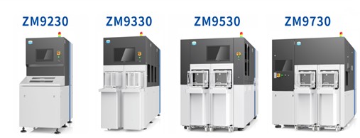
Figure 2 shows four types of high-precision wafer grinding and thinning machines
It is worth mentioning that Chengda Precision Machinery, with its profound technical accumulation and high-level cooperative team, has become the only company in China that simultaneously masters the core technologies and equipment capabilities of laser modification, stripping and grinding. The "Silicon carbide Substrate Laser stripping System" it developed has demonstrated a powerful overall machine processing capability. A large number of experiments have verified that this system has an overwhelming advantage over traditional wire cutting technology in terms of cutting efficiency and material loss. In terms of cutting efficiency, the cutting time for crystal ingots has been significantly reduced to only about 20% of that of traditional wire cutting. Currently, the stripping speed of 8-inch silicon carbide crystal ingots can be controlled within 20 minutes per piece. In terms of material loss, the thickness of the loss layer is less than 80μm, and the yield of 1mm crystal ingots is greater than 2.1 pieces. This system can be adapted to SiC substrate materials of different thicknesses and sizes, integrating full-process functions such as surface grinding and thinning of ingots, laser modification, and complete stripping of wafers, achieving automated and integrated operation. It has greatly promoted cost reduction and efficiency improvement in the silicon carbide industry.

Figure 3 Laser stripping system for silicon carbide substrates
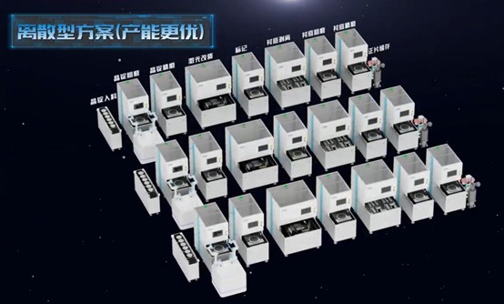
Figure 4 Discrete Solution for Stripping System (with better production capacity)
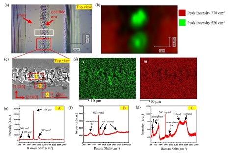
Figure 5 shows the surface structure and morphological characteristics of the stripping and modification area
The company has always adhered to the grand vision of "breaking through the entire chain, intelligently breaking through blockades, and building national chips through chains", with the mission of "breaking through foreign technological blockades and achieving the localization of semiconductor equipment". Relying on the innovative spirit of "not fearing difficulties and striving for the peak", it has been forging ahead on the road of technological innovation in semiconductor equipment. As a national high-tech enterprise, Chengda Precision Machinery has been deeply engaged in the field of precision manufacturing. It has established research institutions such as the Academician Science and Technology Innovation Center and the Doctoral Science and Technology Workstation. It has obtained over 70 authorized patents and more than 20 software Copyrights. Many of its independently developed semiconductor ultra-precision close grinding and polishing process equipment and optical lens full-process equipment have successfully achieved import substitution. The market share remains consistently among the top in the industry. In the future, Chengda Precision Machinery will continue to rely on the deep integration of industry, academia and research, keep making breakthroughs in the field of semiconductor equipment, contribute more to the development of China's semiconductor industry, and lead the industry to new heights!